

What we build
We are building for the part everything else waits for.
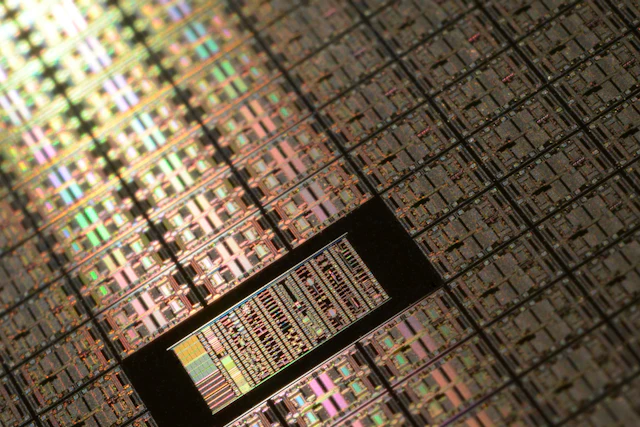
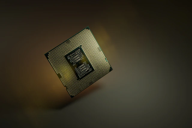
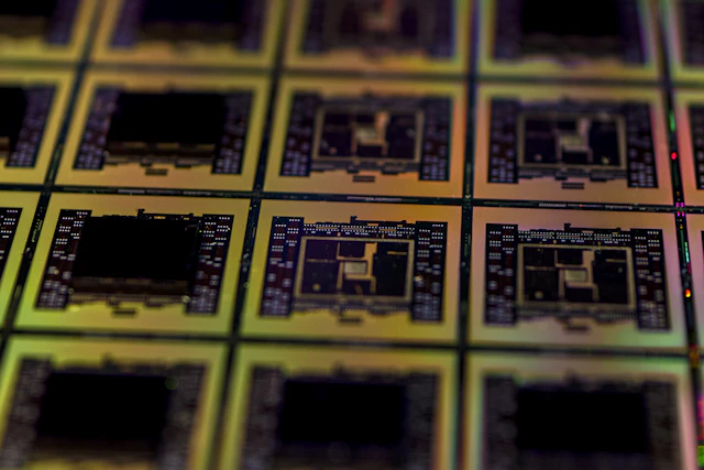
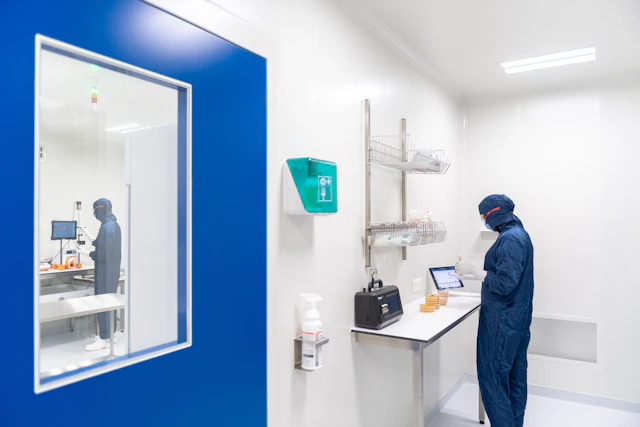
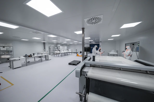
Synthesys is building a semiconductor manufacturing line around one rule: a design should go from tape-out to tested silicon without leaving one line or one record. Designing the chip is half the work. Making it, at yield, in volume, is the half that decides whether a compute roadmap happens on schedule.
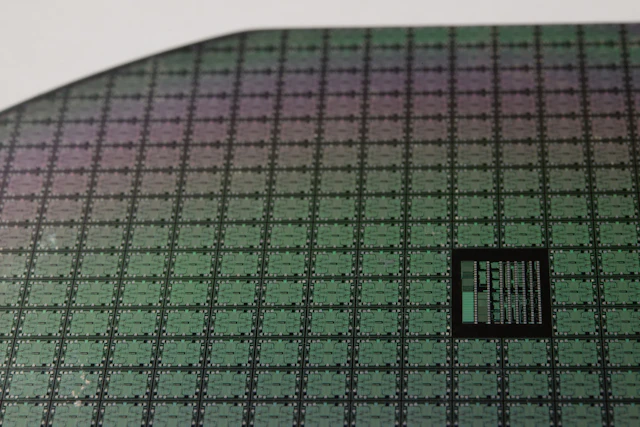
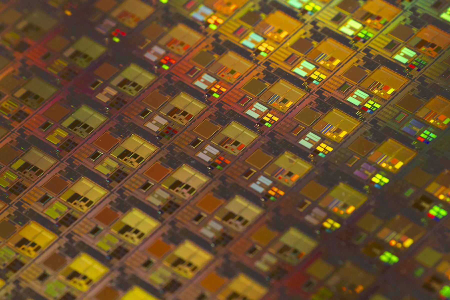
So fabrication, advanced packaging and test are designed to run as a single flow. A wafer that starts here will carry its history with it, through every tool and every step, until it leaves as a part that works. The goal is silicon your team can trust, and a record that shows why.
- Substrate
- 300 mm
- Stage
- Etch
How it will run
Traceable by default
Recipe, tool, chamber and measurement will be written to the lot the moment each step finishes. Nobody has to remember to log it.
One line, not three vendors
Fabrication, packaging and test will share a floor and a schedule. The handoffs that usually cost months become a cart moving between bays.
Yield is an engineering problem
Every excursion will be traced to a cause and closed. You will see the wafer maps and the defect data, so yield is something we work on together.
Built to ramp
The flow that makes your first five wafers will be the flow that makes your first five thousand. Scaling means adding starts, not requalifying.
Limits
Things we do not do.
We do not design chips to sell against our customers. The line will make other people's silicon, and a manufacturer that also competes with you is a conflict you should not have to manage.
We will also not take every job. If a design cannot be made at a yield worth paying for, we will say so before the masks are cut. That will cost us work now and then, and it is why a start date from us will mean something.