

Courses
Not started 02 Chip manufacturing Crystal, cleanroom, lithography, deposition, etch, interconnect 7 lessons
Not started 03 Chip production Tape-out, masks, yield, packaging, chiplets, test, the industry 7 lessons
Not started 04 Chip types CPUs, GPUs, accelerators, FPGAs, memory, SoCs, analog and power 7 lessons
Not started 05 Beyond silicon Compound semiconductors, photonics, new materials, neuromorphic, quantum 7 lessons
Not started
How it works
Start anywhere
The courses build on each other in order, but each one stands alone. If you already know how a transistor works, start at manufacturing.
Short lessons
Every lesson is a five-minute read with the key figures pulled out, so you can come back and check a number without rereading the lesson.
Check yourself
Each course ends with eight questions. Every answer explains why, whether you got it right or not.
Progress stays with you
Your best score is saved in this browser and shown on this page. Nothing is sent to us, and there is no account to create.
Glossary
Twenty words that come up everywhere.
Short definitions for the terms the courses use most. Each one is covered properly in its lesson.
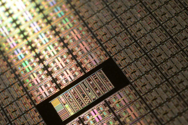
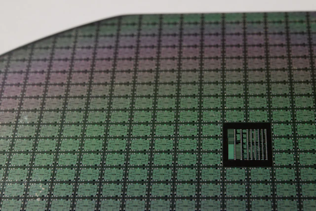
A thin, polished disc of single-crystal silicon, now usually 300 mm across, on which hundreds of chips are built at once.
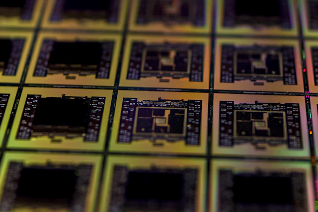
One chip on a wafer, before or after it is cut out. A packaged product may contain one die or many.
An electrically controlled switch. A gate voltage decides whether current flows between source and drain. Modern chips hold billions.
Complementary metal oxide semiconductor: logic built from paired n-type and p-type transistors, so a gate draws real power only while switching.
A name for a manufacturing generation, such as “3 nm”. It no longer measures any feature on the chip.
Transistor shapes in which the gate wraps three sides of a fin (FinFET) or all sides of stacked sheets (gate-all-around), for better control at small sizes.
Printing a circuit pattern onto the wafer with light through a mask, into a light-sensitive resist. It is repeated for every layer.
Extreme ultraviolet lithography, at 13.5 nm wavelength. It prints the finest layers of leading-edge chips in a single exposure where older light needed several.
The mask that holds one layer's pattern. The area a scanner can expose at once, about 26 × 33 mm, caps the size of a single die.
The moment a finished design is handed to manufacturing to make masks. The name dates from when it went on magnetic tape.
The share of dies on a wafer that work. Larger dies and higher defect density both lower it.
A die that has passed test before packaging, so expensive packages are not built around parts that fail.
A smaller die designed to be combined with others in one package, instead of building one very large die.
A layer, often silicon, that sits under several dies and carries dense wiring between them. The basis of 2.5D packaging.
Joining two dies or wafers copper-to-copper and oxide-to-oxide with no solder, at connection pitches of a few micrometres or less.
High-bandwidth memory: DRAM dies stacked vertically and placed next to a processor on an interposer, giving very wide, very fast access.
A company that manufactures chips designed by others. A fabless company designs chips and has a foundry make them.
Outsourced semiconductor assembly and test: companies that package and test chips after the wafer leaves the fab.
The energy needed to free an electron to conduct. It decides how a semiconductor behaves with heat, voltage and light.
The unit of a quantum computer. Unlike a bit, it can hold a superposition of 0 and 1, and qubits can be entangled with one another.